

javanse
-
Posts
15 -
Joined
-
Last visited
javanse's Achievements
")
Newbie (1/14)
0
Reputation
-
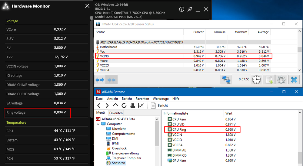
Thanks for the update, build v4337 now correctly shows all eight drives.
-
Here you go: atadump.txt smartdump.txt
-
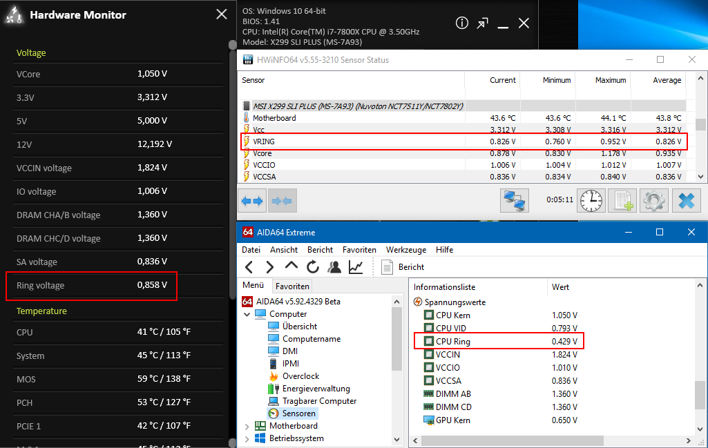
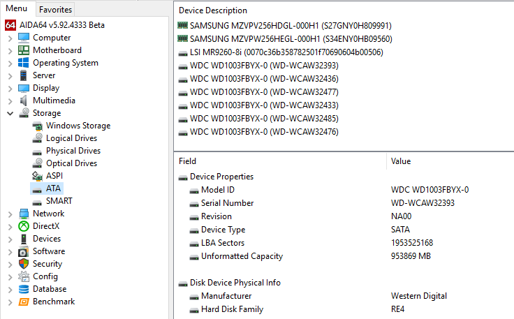
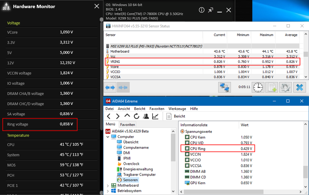
Thanks for the quick update, with build 4333 the vring voltage reading now is correct and in line with MSI CC and HwInfo. All the other voltages were correct from the beginning, so i consider this one about vring as fixed. There's another thing i noticed, completely different topic regarding disk enumeration of RAID arrays: i'm running 8x 1 TB WD RE4 in RAID5 on a LSI 9260-8i controller, but when checking Storage => ATA in AIDA64, only 6 out of 8 drives get listed. raiddump.txt
-
Hi, on my MSI X299 SLI PLUS (MS-7A93), the VRing voltage reading is incorrect, AIDA always shows only half the actual voltage, exactly 50% when compared to MSI Command Center and HwInfo. And fyi: when trying to get the full SMBus reading, the PC insta-rebooted 2 or 3 seconds after the scanning for devices started, so i just took the partial reading. smbusdump_partial.txt isasensordump.txt
-
Ok, if the 32bit interface is intended for now then fine, just wanted to report it as it hit my eye. Another thing: although Fermi cards (400/500 series) could technically support Vulkan, NVidia currently does not enable Vulkan for these GPUs. But as the Vulkan driver 356.39 is officially supported for Fermi, i installed it onto my GTX 470 in my 2nd PC and run both AIDA64 and the Vulkan Caps Viewer on it (the author of that tool is a member of the Vulkan board). Now straight to the bug: AIDA64 does read a lot of Vulkan information for the Fermi GPU where the Vulkan Caps Viewer gives an error message about not being able to create a Vulkan interface. I've talked with the author of Vulkan Caps Viewer about this, and his opinion was that AIDA64 gets its data from the GL<->VK interop without trying to create an actual VkDevice (which would fail on a Fermi GPU at the moment) where his tool tries to create a VkDevice first and then reads the data. Sidenote: VK-Z does the same as AIDA64, i'll give them a bug report too.
-
Thank you for this confirmation, but i'm wondering about the usefulness of a 32bit Vulkan interface. Croteam, the developer of the first game with public Vulkan support "The Talos Principle" stated in their FAQ: Maybe AIDA64 could create an Vulkan interface according to the bit-ness of the Host OS?
-
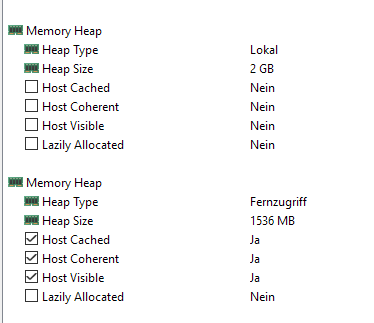
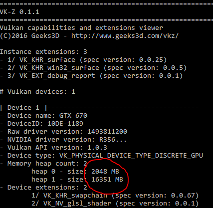
Thanks for the update, the new Vulkan page does display a lot of information on my GTX 670 with 356.39 drivers. Just one thing: it looks like AIDA64 does create a 32bit Vulkan interface only, thus resulting in a Remote Heap Size of only 1,5 GB (see the attached screenshot). I verified this via http://www.geeks3d.com/vkz/ which allows the user to create both 32 and 64bit interfaces, and with VK-Z the 32bit one reads only 1.5 GB remote heap where the 64bit one reads a 16 GB remote heap, matching my installed system ram.
-
Ok that explains why this non-feature is hidden so good. Enjoy your free bug.
-
When using the Video Debug -> Video BIOS Dump feature on UEFI GOP-enabled videocards, the saved files are only ~62kb in size instead of the expected 160-180kb and are corrupted. I tested this with a Gigabyte GTX 670 WF3 with official GOP support and a Zotac GTX 470 with manually added GOP support. When verifying the files produced by AIDA64 with nvflash -v filename.rom the error message is "ERROR: PCI Block corrupted - size mismatch" for both videocards.
-
Thanks for the answer... ...and wow, Vulkan has been released now, that was fast: AMD Vulkan Driver: http://support.amd.com/en-us/kb-articles/Pages/Radeon-Vulkan-Beta.aspx NVIDIA Vulkan Driver: https://developer.nvidia.com/vulkan-driver
-
Hi, now that the new Vulkan API is going to be released in the next days or weeks, i was wondering what will happen to the Mantle Information tab? As the AMD-only Mantle was the starting point for the IHV-independent Vulkan (and thus they're somewhat related), are you planning an update for the Mantle tab to show the Vulkan Information for every supported GPU instead? Afaik the Mantle API already is End-of-Life, so it would make more sense to me to update the Mantle tab to Vulkan than to keep the old Mantle stuff in there.
-
@Pill: You're right and AIDA64 is wrong, i've also reported this some years ago already. @Fiery: What AIDA64 gets wrong: it adds the pagefile to the physical memory and calls it "Swap Space". And then it sums physical memory and "Swap Space" and calls it "Virtual Memory". Pill is correct, rename "Swap Space" to "Commited Memory" (or even "Virtual Memory") and remove the now-current "Virtual Memory" completely. Physical memory + PF = Virtual Memory, there's nothing more to add there.
-
Wrong readings on GeForce GTX Texel Fillrate & System Swap & VM
javanse replied to javanse's topic in Bug reports
Thx Fiery, Build 1251 works fine, i don't have any complaints anymore. -
Wrong readings on GeForce GTX Texel Fillrate & System Swap & VM
javanse replied to javanse's topic in Bug reports
Thanks for the update Fiery, Texel Fillrate reading is now correct But there's another issue related to the TMUs: For my GTX 470, AIDA reads 40 Pixel Pipelines (aka ROPs), which is correct, but also "TMU Per Pipeline = 1", which is wrong in two ways at once. First, it implies 40 while there are 56 TMUs. And second, the item name "TMU Per Pipeline" itself is only correct up to G71. Since G80, ROPs and TMUs are decoupled from each other, so IMHO it should be renamed to "Texture Mapping Units" only as the amount of ROPs is related to the bus width of the memory interface while the amount of TMUs is related to the streaming multiprocessors. Amount of TMUs: 448 Shader / 32 Shader per SM gives 14 SM. Each SM has 4 TMUs for a total of 56 TMUs. Amount of ROPs: 320 bit MI / 64 bit width per ROP-Partition gives 5 ROP-P. Each ROP-P has 8 ROPs for a total of 40 ROPs. kthxbye and a have a nice weekend -
Hi, It looks like AIDA64 uses the wrong formula for calculating the Texel Fillrate for GeForce GTX 400 GPUs, while Pixel Fillrate is calculated correctly. Pixel Fillrate = Core Clock * ROP Count My GTX 470 has 40 ROPs and is clocked @ 750 MHz => 30 GPixel/s, that value is correctly shown by AIDA and GPU-Z. Texel Fillrate = Core Clock * TMU Count My GTX 470 has 56 TMUs and is clocked @ 750 MHz => 42 GTexel/s, that value is correctly shown by GPU-Z while AIDA64 shows exactly 4 times as much, 168 GTexel/s. FYI, this calculation error is visible in all P-States. Second thing, i can't understand some of the readings on the Mainboard -> Memory page. I've 8 GB RAM with a fixed 2 GB min / 2 GB max pagefile which AIDA shows correctly. But it calculates a swap space of 10 GB, apparently RAM+Swap, and 18 GB virtual memory, apparently RAM+swap space, which doesn't make any sense to me. Shouldn't it read a swap space of 2 GB and 10 GB virtual memory, as confirmed by the 10 GB commit charge limit reading from Process Explorer from Sysinternals?